Doc 10 · The Flex Circuits — Wiring That Is Manufactured, Not Cut
Engineered Lighting prototype series · September 2026
PCB build shopping checklist →
The checklist includes the two user-applied mounting adhesives, mating plugs and wires needed alongside these manufactured flexes.
The main board in Doc 9 now consolidates six radial LED sockets into one locking interface. Everything its connectors reach — six ambient zones around a cylinder, three spotlight pairs, two motors — has so far been wire, cut and stripped and soldered by hand, one conductor at a time. These three flexible circuits replace most of that with something a factory makes to a drawing.
The latest main board groups all three spotlight pairs in J9, beside J13 tilt. Ordinary wires connect those plugs to the unchanged static arm ribbon; J12 pan terminates separately. The wire loop across the pan joint must accommodate 180 degrees in each direction. This is not a dynamic-flex qualification. The six spotlight conductors remain separate, including their three LED-minus returns.
They are passive: copper, insulating film and solder pads. No components, no connectors fitted, no firmware. That is the point. A flex circuit is a wiring harness that can be checked before it is built, and reproduced identically the next time.
| Circuit | Design | Size | Copper layers | Pads / contacts | What it does |
|---|---|---|---|---|---|
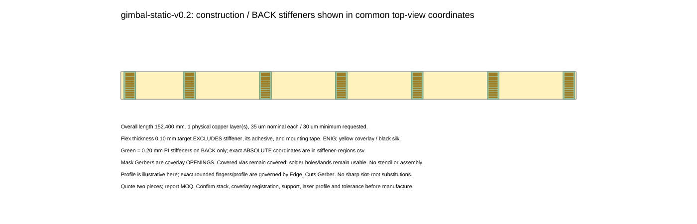
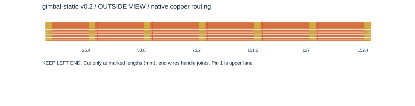
| Arm ribbon | gimbal-static-v0.2 | 152.4 × 9.2 mm | 1 | 70 | Carries motor power, the CAN pair and three spotlight pairs along the arm. Static: it does not flex in service, and ordinary wires cross the moving joints. |
| Upper cylinder band | led-upper-v0.3 | 325.0 × 42.9 mm | 2 | 126 | Connects main J2 directly through a 30-contact insertion tail to six separately fused zones; 96 lands solder to strip ends. |
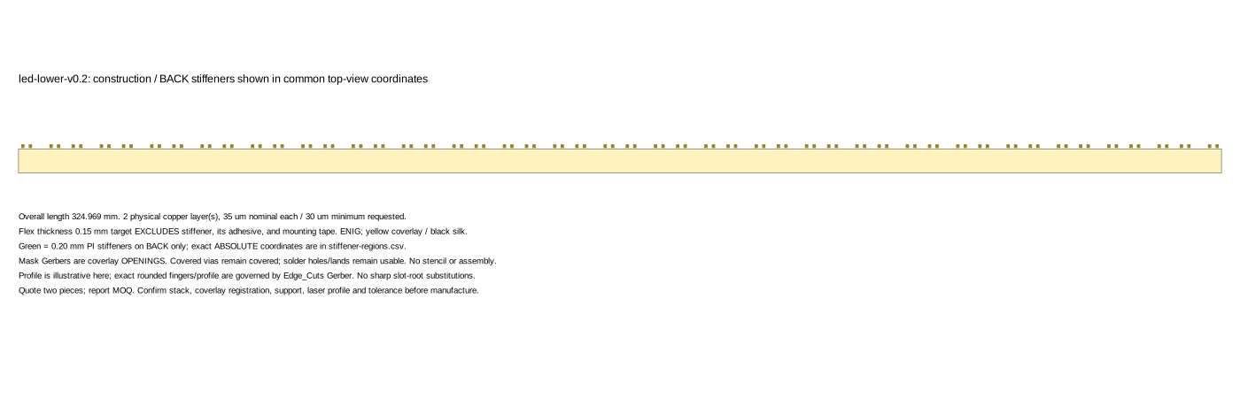
| Lower cylinder band | led-lower-v0.2 | 325.0 × 7.9 mm | 2 | 96 | The mirrored lower band, feeding the same six zones from the other side. |
Status as of 8 September 2026 — submitted for quotation, not built
All three designs pass native electrical-rule and design-rule checks, schematic parity, an independent pin-and-topology oracle, and a comparison of the exported manufacturing data against the native design. Those results are in the table under what has been checked.
Submitted to JLCPCB for engineering quotation; no payment or production release. All three now also have separate PCBWay inquiries. The submitted special requirements preserve the specified 1 oz copper; the website copper, upper-tail support and contact-finish placeholders require engineering correction. The request is two of each circuit, six passive circuits in total, for two fixture prototypes. The manufacturer has not accepted the stack-up, coverlay, stiffeners or tolerances, and there has been no physical qualification of any kind: no fit coupon, no solder sample, no bend or motion testing.
The central-interface main and upper flex v0.3 originally changed together. The later grouped-arm and branding changes affect only the main board; all three flex files remain byte-identical. One continuing fit risk affects whether these can be ordered at all, and it has its own section: the alignment hold.
Words this chapter uses — open this if any of them are new
| Word | What it means here |
|---|---|
| Flex circuit | A printed circuit on a thin plastic film instead of rigid fibreglass, so it can bend or wrap. |
| Polyimide (PI) | The plastic film these are built on. Tough, heat-resistant, and the reason a flex can be soldered at all. |
| Coverlay | The insulating film bonded over the copper, doing the job a solder mask does on a rigid board. Its artwork describes the openings, not the covering. |
| Adhesiveless core | A film with the copper bonded directly to it, without a glue layer. Thinner and better behaved when bent. |
| Stiffener | A local patch of extra material bonded where the circuit must not flex — under a soldered joint, for example. |
| ENIG | Electroless nickel, immersion gold: a flat, solderable, non-tarnishing finish. |
| Rail | One conductor carrying one thing. Here: +24V, and the three white channels W, N and C. |
| Developed length | The length a wrapped band must be cut to so that it fits once curved. Longer than the cylinder's diameter suggests, and sensitive to what it wraps over. |
| Neutral radius | The radius at which the circuit neither stretches nor compresses as it bends. It sets the developed length. |
| Bare circuit | What is being quoted: the circuit alone, with nothing soldered to it. |
The three circuits
Choose a circuit, then turn layers on and off. Hovering or tapping a pad shows what it carries; clicking or tapping pins that summary so you can jump to its row in the connection table.
The flex viewer needs JavaScript. Without it, the construction drawings below show each circuit, and every pad is listed in the connection tables.
What this view shows — and what it does not
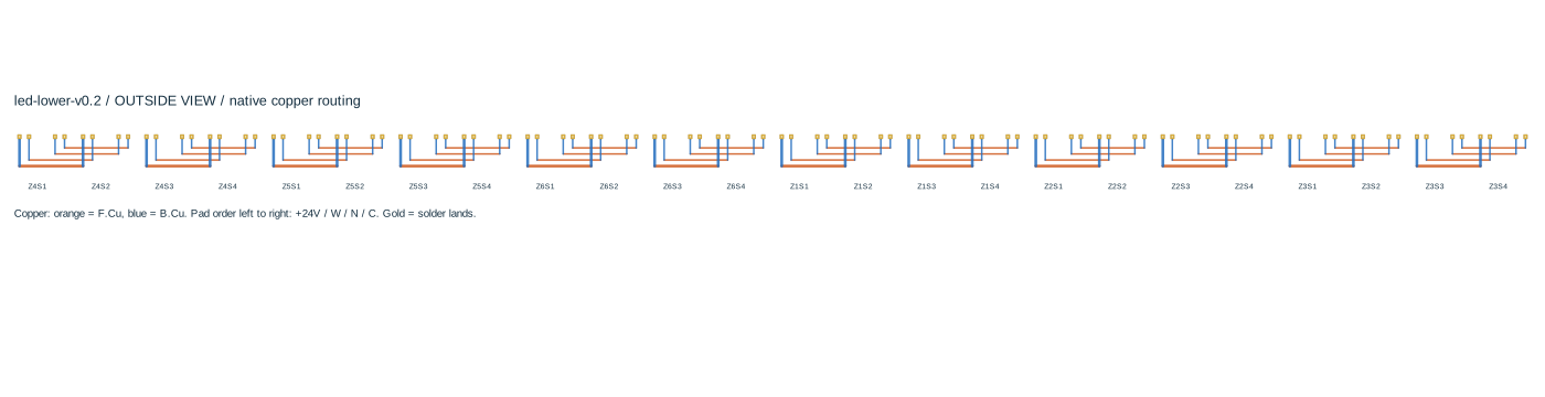
These are the circuits' own manufacturing layers, rendered from the exported artwork: the copper, the coverlay openings and the printed legend. The colours are view colours chosen for contrast, not the colours of the finished part, which is specified as ENIG copper under yellow coverlay with a black legend.
The small round markers are pad locations from each circuit's connection table, not the exact
pad outlines — the real shapes are in the copper and coverlay layers underneath them. On the two
cylinder bands, F.Mask and B.Mask are coverlay openings on a flex circuit, not solder-mask
instructions for a rigid board.
The arm ribbon has one physical copper layer. Its KiCad file shows an empty back-copper layer; that is an editor artefact and must never be ordered as a second layer.
How the wiring is arranged
The arm ribbon
Ten conductors run the length of the arm in parallel lanes: motor +24V and GND on the two widest,
then the CAN_H / CAN_L pair, then three spotlight pairs. Seven termination banks are spaced along
it — the input J1 plus six more — and the ribbon is cut at the marked line for whichever length
the arm needs. Cut lengths of 25.4, 50.8, 76.2, 101.6, 127.0 and 152.4 mm are all verified.
It is static. It does not flex while the fixture moves; ordinary wires with service loops cross the moving joints, exactly as Doc 1's rule requires. No repeated-motion qualification is claimed, because none is needed and none has been done.
The two cylinder bands
Each band wraps the cylinder and feeds six ambient zones, four rails each. The flat zone order is Z4, Z5, Z6, Z1, Z2, Z3, which puts the seam between Z3 and Z4 and the input tab between Z6 and Z1 — away from the common connection area, so one tab can feed three zones in each direction. All four rails are parallel-load interconnects. They are never a series string, and the six fused feeds from the main board stay separate the whole way.
Where a band meets an LED strip, the copper finger overlaps the strip's own end pad by a nominal 1 mm, with a 0.3 mm plated hole through the joint for solder access and anchoring. That hole is not a connector socket.
The tail is the plug
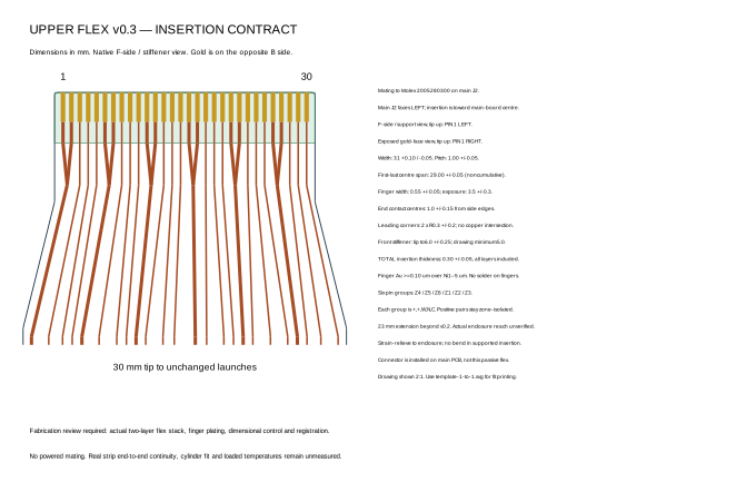
Upper v0.3 (0af25f8f) replaces the v0.2 wire-solder tab. The gold fingers on
the back face slide directly into main J2; they are not pads for soldering wires.
The rigid main remains inside the cylinder while the flexible band wraps around
it. Keep the tail long enough to reach and bend gently: the overall upper board
height is 42.9 mm, including 35 mm above the band's upper edge. Do not crease the
stiffened insertion section or shorten it based on the old solder-pad picture.
The connector uses thirty 1 mm-pitch contacts, grouped in zone order 4, 5, 6, 1, 2, 3, with +,+,W,N,C in each group. The front stiffener is opposite the back gold contacts. The required 0.30 ±0.05 mm is the total insertion thickness, including copper, film, plating, adhesive and support. Finger gold requires at least 0.10 µm over nickel; ordinary 2 microinch ENIG is not the same specification. Exact tip exposure, coverlay and stack need supplier review. These are fabrication requirements, not measured dimensions.
The 96 strip-end lands and retained band routes did not change. Some outer strip lands still look isolated when only the upper flex is viewed: the intended path continues through matching rails inside the real strip, into a lower-band bridge and up the next strip. The independent installed-CAM model reaches all 192 strip ends on the correct 24 rails only if those real through-rails exist. Check them unpowered; net labels alone cannot prove the assembled path.
An isolated current-tail/contact screen predicts a worst loop drop of 0.1044 V under assumed 85 °C copper, 30 µm copper thickness, reduced conductor widths and the stated connector resistance. It excludes the rest of the LED circuit and does not predict heating. The 0.60 A positive / 0.20 A channel cases are stress screens, not continuous operating ratings. Initial commissioning remains at most 0.50 A RMS per radial zone with local fuse air at most 85 °C, subject to measured loads and PWM duty limits. Actual temperatures and currents are unknown.
The alignment hold — still a fabrication gate
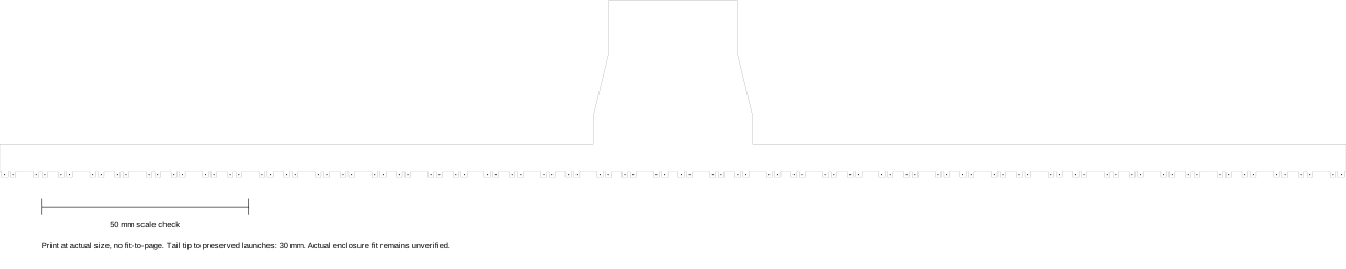
Print the template and dry-fit before anything is fabricated
The bands are positioned against a modelled cylinder: a neutral radius of 51.975 mm and a developed length of 324.97 mm, giving a 13.607 mm pitch across 24 strips. Underneath them sits 1.1 mm double-sided adhesive whose datasheet allows a typical ±10 % thickness tolerance.
That tolerance alone moves the far-end pad alignment by up to 0.346 mm over half a turn, against a nominal lateral copper margin of 0.30 mm each side — before any fabrication or assembly error is added. The measured strip is also 0.7 mm thick without a specified copper neutral radius or facet shape, so the real mounted curve is not established.
Use the current upper template-1-to-1.svg from the downloads at actual size and check its scale. The retained A3 PDF is historical v0.2: its upper-tail drawing is obsolete and cannot qualify the new insertion fit. Its unchanged lower/arm portions remain reference material. Dry-fit every pad position on the actual compressed stack. If the alignment misses, measure that stack and regenerate the geometry — do not stretch the circuit, and do not approve fabrication. This is a known sensitivity, not a passed physical test.
What the copper loses
The full-path table below is historical, calculated with upper v0.2 (a5acd2a0), not the new
insertion tail. The lower and arm geometry has not changed. Keep these earlier sensitivity results
for their reasoning; do not use their full-loop totals to qualify the current assembly. They include
assumed strip through-rails and joints, exclude the controller and external cabling, and are not measurements.
| Sensitivity case | Worst LED strip supply loss | Gimbal motor loop | Each spotlight pair | Assumed copper temperature | Assumed copper |
|---|---|---|---|---|---|
| Historical upper v0.2: nominal model | 0.342 V | 0.094 V | 0.091 V | 20 °C | 35 µm |
| Historical upper v0.2: hot/thin screening | 0.583 V | 0.137 V | 0.133 V | 85 °C | 30 µm |
| Historical upper v0.2: high-resistance joints sensitivity | 0.903 V | 0.137 V | 0.133 V | 85 °C | 30 µm |
The project's wiring budget is 3 % of 24 V, which is 0.72 V for the whole path — not just for these circuits. The historical nominal case was inside it; the historical high-resistance-joint sensitivity was not, which is the point of including it. A bad solder joint is a repair, not a tolerance to design around: measure the loaded voltage and fix the joint.
Temperatures in that table are inputs, not predictions. Copper loss and actual bonded temperature have to be checked during the first powered tests.
Building and installing them
The engineering notes linked below summarize the current construction and open checks. The steps that most affect whether this works:
- Check the cut segment unpowered first. Matching
+24V/W/N/Clabels must conduct end to end, and no component may encroach on the joint. - The outside view is authoritative when wrapping. The lower band's artwork already points its fingers upward; do not mirror it to match the upper band.
- Make a supported sample joint before committing. Pre-tin lightly, support the finger, and check both interfaces wet without bridging.
- Foam goes on band backs only, stopping 0.7 mm short of the finger roots, and never under a strip body. Form gently: no crease, and no repeated bend at a via, a solder land or a stiffener edge.
- Before power, compare the delivered netlist and check every pair for isolation. After the strips are connected, expect 24 isolated zone rails. Use a low-voltage continuity test, not a high-voltage insulation tester, across populated LEDs. Confirm no rail reaches the aluminium.
- Power one zone at a time, then measure full-load voltage drop, current and temperature.
Every pad, and what it carries
Each row is one strip/ribbon solder pad or one of the thirty J100 insertion contacts. Selecting a pad in the viewer marks its row here; the summary's button scrolls to it.
Arm ribbon 70 pads
| Reference | Pin | Carries | Role | Position (mm) |
|---|---|---|---|---|
| J6 | 1 | V24_MOTOR2 | 144.60, 20.95 | |
| J6 | 2 | GND | 144.60, 22.35 | |
| J6 | 3 | CAN_H | 144.60, 23.40 | |
| J6 | 4 | CAN_L | 144.60, 24.10 | |
| J6 | 5 | SPOT1_LED_PLUS | 144.60, 24.82 | |
| J6 | 6 | SPOT1_LED_MINUS | 144.60, 25.57 | |
| J6 | 7 | SPOT2_LED_PLUS | 144.60, 26.32 | |
| J6 | 8 | SPOT2_LED_MINUS | 144.60, 27.07 | |
| J6 | 9 | SPOT3_LED_PLUS | 144.60, 27.82 | |
| J6 | 10 | SPOT3_LED_MINUS | 144.60, 28.57 | |
| J3 | 1 | V24_MOTOR2 | 68.40, 20.95 | |
| J3 | 2 | GND | 68.40, 22.35 | |
| J3 | 3 | CAN_H | 68.40, 23.40 | |
| J3 | 4 | CAN_L | 68.40, 24.10 | |
| J3 | 5 | SPOT1_LED_PLUS | 68.40, 24.82 | |
| J3 | 6 | SPOT1_LED_MINUS | 68.40, 25.57 | |
| J3 | 7 | SPOT2_LED_PLUS | 68.40, 26.32 | |
| J3 | 8 | SPOT2_LED_MINUS | 68.40, 27.07 | |
| J3 | 9 | SPOT3_LED_PLUS | 68.40, 27.82 | |
| J3 | 10 | SPOT3_LED_MINUS | 68.40, 28.57 | |
| J2 | 1 | V24_MOTOR2 | 43.00, 20.95 | |
| J2 | 2 | GND | 43.00, 22.35 | |
| J2 | 3 | CAN_H | 43.00, 23.40 | |
| J2 | 4 | CAN_L | 43.00, 24.10 | |
| J2 | 5 | SPOT1_LED_PLUS | 43.00, 24.82 | |
| J2 | 6 | SPOT1_LED_MINUS | 43.00, 25.57 | |
| J2 | 7 | SPOT2_LED_PLUS | 43.00, 26.32 | |
| J2 | 8 | SPOT2_LED_MINUS | 43.00, 27.07 | |
| J2 | 9 | SPOT3_LED_PLUS | 43.00, 27.82 | |
| J2 | 10 | SPOT3_LED_MINUS | 43.00, 28.57 | |
| J4 | 1 | V24_MOTOR2 | 93.80, 20.95 | |
| J4 | 2 | GND | 93.80, 22.35 | |
| J4 | 3 | CAN_H | 93.80, 23.40 | |
| J4 | 4 | CAN_L | 93.80, 24.10 | |
| J4 | 5 | SPOT1_LED_PLUS | 93.80, 24.82 | |
| J4 | 6 | SPOT1_LED_MINUS | 93.80, 25.57 | |
| J4 | 7 | SPOT2_LED_PLUS | 93.80, 26.32 | |
| J4 | 8 | SPOT2_LED_MINUS | 93.80, 27.07 | |
| J4 | 9 | SPOT3_LED_PLUS | 93.80, 27.82 | |
| J4 | 10 | SPOT3_LED_MINUS | 93.80, 28.57 | |
| J5 | 1 | V24_MOTOR2 | 119.20, 20.95 | |
| J5 | 2 | GND | 119.20, 22.35 | |
| J5 | 3 | CAN_H | 119.20, 23.40 | |
| J5 | 4 | CAN_L | 119.20, 24.10 | |
| J5 | 5 | SPOT1_LED_PLUS | 119.20, 24.82 | |
| J5 | 6 | SPOT1_LED_MINUS | 119.20, 25.57 | |
| J5 | 7 | SPOT2_LED_PLUS | 119.20, 26.32 | |
| J5 | 8 | SPOT2_LED_MINUS | 119.20, 27.07 | |
| J5 | 9 | SPOT3_LED_PLUS | 119.20, 27.82 | |
| J5 | 10 | SPOT3_LED_MINUS | 119.20, 28.57 | |
| J7 | 1 | V24_MOTOR2 | 170.00, 20.95 | |
| J7 | 2 | GND | 170.00, 22.35 | |
| J7 | 3 | CAN_H | 170.00, 23.40 | |
| J7 | 4 | CAN_L | 170.00, 24.10 | |
| J7 | 5 | SPOT1_LED_PLUS | 170.00, 24.82 | |
| J7 | 6 | SPOT1_LED_MINUS | 170.00, 25.57 | |
| J7 | 7 | SPOT2_LED_PLUS | 170.00, 26.32 | |
| J7 | 8 | SPOT2_LED_MINUS | 170.00, 27.07 | |
| J7 | 9 | SPOT3_LED_PLUS | 170.00, 27.82 | |
| J7 | 10 | SPOT3_LED_MINUS | 170.00, 28.57 | |
| J1 | 1 | V24_MOTOR2 | 23.00, 20.95 | |
| J1 | 2 | GND | 23.00, 22.35 | |
| J1 | 3 | CAN_H | 23.00, 23.40 | |
| J1 | 4 | CAN_L | 23.00, 24.10 | |
| J1 | 5 | SPOT1_LED_PLUS | 23.00, 24.82 | |
| J1 | 6 | SPOT1_LED_MINUS | 23.00, 25.57 | |
| J1 | 7 | SPOT2_LED_PLUS | 23.00, 26.32 | |
| J1 | 8 | SPOT2_LED_MINUS | 23.00, 27.07 | |
| J1 | 9 | SPOT3_LED_PLUS | 23.00, 27.82 | |
| J1 | 10 | SPOT3_LED_MINUS | 23.00, 28.57 |
Upper cylinder band 126 pads
| Reference | Pin | Carries | Role | Position (mm) |
|---|---|---|---|---|
| J43 | 1 | Z4_T23_24V | strip solder overlap | 48.39, 47.20 |
| J43 | 2 | Z4_T23_W | strip solder overlap | 50.42, 47.20 |
| J43 | 3 | Z4_T23_N | strip solder overlap | 56.01, 47.20 |
| J43 | 4 | Z4_T23_C | strip solder overlap | 58.04, 47.20 |
| J64 | 1 | ZONE6_24V | strip solder overlap | 170.85, 47.20 |
| J64 | 2 | ZONE6_W | strip solder overlap | 172.89, 47.20 |
| J64 | 3 | ZONE6_N | strip solder overlap | 178.48, 47.20 |
| J64 | 4 | ZONE6_C | strip solder overlap | 180.51, 47.20 |
| J41 | 1 | unconnected-(J41-Pin_1-Pad1) | strip solder overlap | 21.18, 47.20 |
| J41 | 2 | unconnected-(J41-Pin_2-Pad2) | strip solder overlap | 23.21, 47.20 |
| J41 | 3 | unconnected-(J41-Pin_3-Pad3) | strip solder overlap | 28.80, 47.20 |
| J41 | 4 | unconnected-(J41-Pin_4-Pad4) | strip solder overlap | 30.83, 47.20 |
| J12 | 1 | Z1_T23_24V | strip solder overlap | 198.07, 47.20 |
| J12 | 2 | Z1_T23_W | strip solder overlap | 200.10, 47.20 |
| J12 | 3 | Z1_T23_N | strip solder overlap | 205.69, 47.20 |
| J12 | 4 | Z1_T23_C | strip solder overlap | 207.72, 47.20 |
| J14 | 1 | unconnected-(J14-Pin_1-Pad1) | strip solder overlap | 225.28, 47.20 |
| J14 | 2 | unconnected-(J14-Pin_2-Pad2) | strip solder overlap | 227.31, 47.20 |
| J14 | 3 | unconnected-(J14-Pin_3-Pad3) | strip solder overlap | 232.90, 47.20 |
| J14 | 4 | unconnected-(J14-Pin_4-Pad4) | strip solder overlap | 234.94, 47.20 |
| J21 | 1 | ZONE2_24V | strip solder overlap | 238.89, 47.20 |
| J21 | 2 | ZONE2_W | strip solder overlap | 240.92, 47.20 |
| J21 | 3 | ZONE2_N | strip solder overlap | 246.51, 47.20 |
| J21 | 4 | ZONE2_C | strip solder overlap | 248.54, 47.20 |
| J51 | 1 | unconnected-(J51-Pin_1-Pad1) | strip solder overlap | 75.61, 47.20 |
| J51 | 2 | unconnected-(J51-Pin_2-Pad2) | strip solder overlap | 77.64, 47.20 |
| J51 | 3 | unconnected-(J51-Pin_3-Pad3) | strip solder overlap | 83.23, 47.20 |
| J51 | 4 | unconnected-(J51-Pin_4-Pad4) | strip solder overlap | 85.26, 47.20 |
| J52 | 1 | Z5_T23_24V | strip solder overlap | 89.21, 47.20 |
| J52 | 2 | Z5_T23_W | strip solder overlap | 91.24, 47.20 |
| J52 | 3 | Z5_T23_N | strip solder overlap | 96.83, 47.20 |
| J52 | 4 | Z5_T23_C | strip solder overlap | 98.87, 47.20 |
| J11 | 1 | ZONE1_24V | strip solder overlap | 184.46, 47.20 |
| J11 | 2 | ZONE1_W | strip solder overlap | 186.49, 47.20 |
| J11 | 3 | ZONE1_N | strip solder overlap | 192.08, 47.20 |
| J11 | 4 | ZONE1_C | strip solder overlap | 194.11, 47.20 |
| J54 | 1 | ZONE5_24V | strip solder overlap | 116.43, 47.20 |
| J54 | 2 | ZONE5_W | strip solder overlap | 118.46, 47.20 |
| J54 | 3 | ZONE5_N | strip solder overlap | 124.05, 47.20 |
| J54 | 4 | ZONE5_C | strip solder overlap | 126.08, 47.20 |
| J42 | 1 | Z4_T23_24V | strip solder overlap | 34.78, 47.20 |
| J42 | 2 | Z4_T23_W | strip solder overlap | 36.82, 47.20 |
| J42 | 3 | Z4_T23_N | strip solder overlap | 42.40, 47.20 |
| J42 | 4 | Z4_T23_C | strip solder overlap | 44.44, 47.20 |
| J100 | 1 | ZONE4_24V | B-side insertion contact; no solder | 167.98, 6.75 |
| J100 | 2 | ZONE4_24V | B-side insertion contact; no solder | 168.98, 6.75 |
| J100 | 3 | ZONE4_W | B-side insertion contact; no solder | 169.98, 6.75 |
| J100 | 4 | ZONE4_N | B-side insertion contact; no solder | 170.98, 6.75 |
| J100 | 5 | ZONE4_C | B-side insertion contact; no solder | 171.98, 6.75 |
| J100 | 6 | ZONE5_24V | B-side insertion contact; no solder | 172.98, 6.75 |
| J100 | 7 | ZONE5_24V | B-side insertion contact; no solder | 173.98, 6.75 |
| J100 | 8 | ZONE5_W | B-side insertion contact; no solder | 174.98, 6.75 |
| J100 | 9 | ZONE5_N | B-side insertion contact; no solder | 175.98, 6.75 |
| J100 | 10 | ZONE5_C | B-side insertion contact; no solder | 176.98, 6.75 |
| J100 | 11 | ZONE6_24V | B-side insertion contact; no solder | 177.98, 6.75 |
| J100 | 12 | ZONE6_24V | B-side insertion contact; no solder | 178.98, 6.75 |
| J100 | 13 | ZONE6_W | B-side insertion contact; no solder | 179.98, 6.75 |
| J100 | 14 | ZONE6_N | B-side insertion contact; no solder | 180.98, 6.75 |
| J100 | 15 | ZONE6_C | B-side insertion contact; no solder | 181.98, 6.75 |
| J100 | 16 | ZONE1_24V | B-side insertion contact; no solder | 182.98, 6.75 |
| J100 | 17 | ZONE1_24V | B-side insertion contact; no solder | 183.98, 6.75 |
| J100 | 18 | ZONE1_W | B-side insertion contact; no solder | 184.98, 6.75 |
| J100 | 19 | ZONE1_N | B-side insertion contact; no solder | 185.98, 6.75 |
| J100 | 20 | ZONE1_C | B-side insertion contact; no solder | 186.98, 6.75 |
| J100 | 21 | ZONE2_24V | B-side insertion contact; no solder | 187.98, 6.75 |
| J100 | 22 | ZONE2_24V | B-side insertion contact; no solder | 188.98, 6.75 |
| J100 | 23 | ZONE2_W | B-side insertion contact; no solder | 189.98, 6.75 |
| J100 | 24 | ZONE2_N | B-side insertion contact; no solder | 190.98, 6.75 |
| J100 | 25 | ZONE2_C | B-side insertion contact; no solder | 191.98, 6.75 |
| J100 | 26 | ZONE3_24V | B-side insertion contact; no solder | 192.98, 6.75 |
| J100 | 27 | ZONE3_24V | B-side insertion contact; no solder | 193.98, 6.75 |
| J100 | 28 | ZONE3_W | B-side insertion contact; no solder | 194.98, 6.75 |
| J100 | 29 | ZONE3_N | B-side insertion contact; no solder | 195.98, 6.75 |
| J100 | 30 | ZONE3_C | B-side insertion contact; no solder | 196.98, 6.75 |
| J22 | 1 | Z2_T23_24V | strip solder overlap | 252.50, 47.20 |
| J22 | 2 | Z2_T23_W | strip solder overlap | 254.53, 47.20 |
| J22 | 3 | Z2_T23_N | strip solder overlap | 260.12, 47.20 |
| J22 | 4 | Z2_T23_C | strip solder overlap | 262.15, 47.20 |
| J34 | 1 | unconnected-(J34-Pin_1-Pad1) | strip solder overlap | 334.14, 47.20 |
| J34 | 2 | unconnected-(J34-Pin_2-Pad2) | strip solder overlap | 336.17, 47.20 |
| J34 | 3 | unconnected-(J34-Pin_3-Pad3) | strip solder overlap | 341.76, 47.20 |
| J34 | 4 | unconnected-(J34-Pin_4-Pad4) | strip solder overlap | 343.79, 47.20 |
| J44 | 1 | ZONE4_24V | strip solder overlap | 62.00, 47.20 |
| J44 | 2 | ZONE4_W | strip solder overlap | 64.03, 47.20 |
| J44 | 3 | ZONE4_N | strip solder overlap | 69.62, 47.20 |
| J44 | 4 | ZONE4_C | strip solder overlap | 71.65, 47.20 |
| J32 | 1 | Z3_T23_24V | strip solder overlap | 306.92, 47.20 |
| J32 | 2 | Z3_T23_W | strip solder overlap | 308.96, 47.20 |
| J32 | 3 | Z3_T23_N | strip solder overlap | 314.55, 47.20 |
| J32 | 4 | Z3_T23_C | strip solder overlap | 316.58, 47.20 |
| J53 | 1 | Z5_T23_24V | strip solder overlap | 102.82, 47.20 |
| J53 | 2 | Z5_T23_W | strip solder overlap | 104.85, 47.20 |
| J53 | 3 | Z5_T23_N | strip solder overlap | 110.44, 47.20 |
| J53 | 4 | Z5_T23_C | strip solder overlap | 112.47, 47.20 |
| J23 | 1 | Z2_T23_24V | strip solder overlap | 266.10, 47.20 |
| J23 | 2 | Z2_T23_W | strip solder overlap | 268.14, 47.20 |
| J23 | 3 | Z2_T23_N | strip solder overlap | 273.72, 47.20 |
| J23 | 4 | Z2_T23_C | strip solder overlap | 275.76, 47.20 |
| J62 | 1 | Z6_T23_24V | strip solder overlap | 143.64, 47.20 |
| J62 | 2 | Z6_T23_W | strip solder overlap | 145.67, 47.20 |
| J62 | 3 | Z6_T23_N | strip solder overlap | 151.26, 47.20 |
| J62 | 4 | Z6_T23_C | strip solder overlap | 153.29, 47.20 |
| J24 | 1 | unconnected-(J24-Pin_1-Pad1) | strip solder overlap | 279.71, 47.20 |
| J24 | 2 | unconnected-(J24-Pin_2-Pad2) | strip solder overlap | 281.74, 47.20 |
| J24 | 3 | unconnected-(J24-Pin_3-Pad3) | strip solder overlap | 287.33, 47.20 |
| J24 | 4 | unconnected-(J24-Pin_4-Pad4) | strip solder overlap | 289.36, 47.20 |
| J63 | 1 | Z6_T23_24V | strip solder overlap | 157.25, 47.20 |
| J63 | 2 | Z6_T23_W | strip solder overlap | 159.28, 47.20 |
| J63 | 3 | Z6_T23_N | strip solder overlap | 164.87, 47.20 |
| J63 | 4 | Z6_T23_C | strip solder overlap | 166.90, 47.20 |
| J33 | 1 | Z3_T23_24V | strip solder overlap | 320.53, 47.20 |
| J33 | 2 | Z3_T23_W | strip solder overlap | 322.56, 47.20 |
| J33 | 3 | Z3_T23_N | strip solder overlap | 328.15, 47.20 |
| J33 | 4 | Z3_T23_C | strip solder overlap | 330.18, 47.20 |
| J13 | 1 | Z1_T23_24V | strip solder overlap | 211.68, 47.20 |
| J13 | 2 | Z1_T23_W | strip solder overlap | 213.71, 47.20 |
| J13 | 3 | Z1_T23_N | strip solder overlap | 219.30, 47.20 |
| J13 | 4 | Z1_T23_C | strip solder overlap | 221.33, 47.20 |
| J31 | 1 | ZONE3_24V | strip solder overlap | 293.32, 47.20 |
| J31 | 2 | ZONE3_W | strip solder overlap | 295.35, 47.20 |
| J31 | 3 | ZONE3_N | strip solder overlap | 300.94, 47.20 |
| J31 | 4 | ZONE3_C | strip solder overlap | 302.97, 47.20 |
| J61 | 1 | unconnected-(J61-Pin_1-Pad1) | strip solder overlap | 130.03, 47.20 |
| J61 | 2 | unconnected-(J61-Pin_2-Pad2) | strip solder overlap | 132.07, 47.20 |
| J61 | 3 | unconnected-(J61-Pin_3-Pad3) | strip solder overlap | 137.65, 47.20 |
| J61 | 4 | unconnected-(J61-Pin_4-Pad4) | strip solder overlap | 139.69, 47.20 |
Lower cylinder band 96 pads
| Reference | Pin | Carries | Role | Position (mm) |
|---|---|---|---|---|
| J41 | 1 | Z4_B12_24V | strip solder overlap | 21.18, 39.20 |
| J41 | 2 | Z4_B12_W | strip solder overlap | 23.21, 39.20 |
| J41 | 3 | Z4_B12_N | strip solder overlap | 28.80, 39.20 |
| J41 | 4 | Z4_B12_C | strip solder overlap | 30.83, 39.20 |
| J42 | 1 | Z4_B12_24V | strip solder overlap | 34.78, 39.20 |
| J42 | 2 | Z4_B12_W | strip solder overlap | 36.82, 39.20 |
| J42 | 3 | Z4_B12_N | strip solder overlap | 42.40, 39.20 |
| J42 | 4 | Z4_B12_C | strip solder overlap | 44.44, 39.20 |
| J43 | 1 | Z4_B34_24V | strip solder overlap | 48.39, 39.20 |
| J43 | 2 | Z4_B34_W | strip solder overlap | 50.42, 39.20 |
| J43 | 3 | Z4_B34_N | strip solder overlap | 56.01, 39.20 |
| J43 | 4 | Z4_B34_C | strip solder overlap | 58.04, 39.20 |
| J44 | 1 | Z4_B34_24V | strip solder overlap | 62.00, 39.20 |
| J44 | 2 | Z4_B34_W | strip solder overlap | 64.03, 39.20 |
| J44 | 3 | Z4_B34_N | strip solder overlap | 69.62, 39.20 |
| J44 | 4 | Z4_B34_C | strip solder overlap | 71.65, 39.20 |
| J51 | 1 | Z5_B12_24V | strip solder overlap | 75.61, 39.20 |
| J51 | 2 | Z5_B12_W | strip solder overlap | 77.64, 39.20 |
| J51 | 3 | Z5_B12_N | strip solder overlap | 83.23, 39.20 |
| J51 | 4 | Z5_B12_C | strip solder overlap | 85.26, 39.20 |
| J52 | 1 | Z5_B12_24V | strip solder overlap | 89.21, 39.20 |
| J52 | 2 | Z5_B12_W | strip solder overlap | 91.24, 39.20 |
| J52 | 3 | Z5_B12_N | strip solder overlap | 96.83, 39.20 |
| J52 | 4 | Z5_B12_C | strip solder overlap | 98.87, 39.20 |
| J53 | 1 | Z5_B34_24V | strip solder overlap | 102.82, 39.20 |
| J53 | 2 | Z5_B34_W | strip solder overlap | 104.85, 39.20 |
| J53 | 3 | Z5_B34_N | strip solder overlap | 110.44, 39.20 |
| J53 | 4 | Z5_B34_C | strip solder overlap | 112.47, 39.20 |
| J54 | 1 | Z5_B34_24V | strip solder overlap | 116.43, 39.20 |
| J54 | 2 | Z5_B34_W | strip solder overlap | 118.46, 39.20 |
| J54 | 3 | Z5_B34_N | strip solder overlap | 124.05, 39.20 |
| J54 | 4 | Z5_B34_C | strip solder overlap | 126.08, 39.20 |
| J61 | 1 | Z6_B12_24V | strip solder overlap | 130.03, 39.20 |
| J61 | 2 | Z6_B12_W | strip solder overlap | 132.07, 39.20 |
| J61 | 3 | Z6_B12_N | strip solder overlap | 137.65, 39.20 |
| J61 | 4 | Z6_B12_C | strip solder overlap | 139.69, 39.20 |
| J62 | 1 | Z6_B12_24V | strip solder overlap | 143.64, 39.20 |
| J62 | 2 | Z6_B12_W | strip solder overlap | 145.67, 39.20 |
| J62 | 3 | Z6_B12_N | strip solder overlap | 151.26, 39.20 |
| J62 | 4 | Z6_B12_C | strip solder overlap | 153.29, 39.20 |
| J63 | 1 | Z6_B34_24V | strip solder overlap | 157.25, 39.20 |
| J63 | 2 | Z6_B34_W | strip solder overlap | 159.28, 39.20 |
| J63 | 3 | Z6_B34_N | strip solder overlap | 164.87, 39.20 |
| J63 | 4 | Z6_B34_C | strip solder overlap | 166.90, 39.20 |
| J64 | 1 | Z6_B34_24V | strip solder overlap | 170.85, 39.20 |
| J64 | 2 | Z6_B34_W | strip solder overlap | 172.89, 39.20 |
| J64 | 3 | Z6_B34_N | strip solder overlap | 178.48, 39.20 |
| J64 | 4 | Z6_B34_C | strip solder overlap | 180.51, 39.20 |
| J11 | 1 | Z1_B12_24V | strip solder overlap | 184.46, 39.20 |
| J11 | 2 | Z1_B12_W | strip solder overlap | 186.49, 39.20 |
| J11 | 3 | Z1_B12_N | strip solder overlap | 192.08, 39.20 |
| J11 | 4 | Z1_B12_C | strip solder overlap | 194.11, 39.20 |
| J12 | 1 | Z1_B12_24V | strip solder overlap | 198.07, 39.20 |
| J12 | 2 | Z1_B12_W | strip solder overlap | 200.10, 39.20 |
| J12 | 3 | Z1_B12_N | strip solder overlap | 205.69, 39.20 |
| J12 | 4 | Z1_B12_C | strip solder overlap | 207.72, 39.20 |
| J13 | 1 | Z1_B34_24V | strip solder overlap | 211.68, 39.20 |
| J13 | 2 | Z1_B34_W | strip solder overlap | 213.71, 39.20 |
| J13 | 3 | Z1_B34_N | strip solder overlap | 219.30, 39.20 |
| J13 | 4 | Z1_B34_C | strip solder overlap | 221.33, 39.20 |
| J14 | 1 | Z1_B34_24V | strip solder overlap | 225.28, 39.20 |
| J14 | 2 | Z1_B34_W | strip solder overlap | 227.31, 39.20 |
| J14 | 3 | Z1_B34_N | strip solder overlap | 232.90, 39.20 |
| J14 | 4 | Z1_B34_C | strip solder overlap | 234.94, 39.20 |
| J21 | 1 | Z2_B12_24V | strip solder overlap | 238.89, 39.20 |
| J21 | 2 | Z2_B12_W | strip solder overlap | 240.92, 39.20 |
| J21 | 3 | Z2_B12_N | strip solder overlap | 246.51, 39.20 |
| J21 | 4 | Z2_B12_C | strip solder overlap | 248.54, 39.20 |
| J22 | 1 | Z2_B12_24V | strip solder overlap | 252.50, 39.20 |
| J22 | 2 | Z2_B12_W | strip solder overlap | 254.53, 39.20 |
| J22 | 3 | Z2_B12_N | strip solder overlap | 260.12, 39.20 |
| J22 | 4 | Z2_B12_C | strip solder overlap | 262.15, 39.20 |
| J23 | 1 | Z2_B34_24V | strip solder overlap | 266.10, 39.20 |
| J23 | 2 | Z2_B34_W | strip solder overlap | 268.14, 39.20 |
| J23 | 3 | Z2_B34_N | strip solder overlap | 273.72, 39.20 |
| J23 | 4 | Z2_B34_C | strip solder overlap | 275.76, 39.20 |
| J24 | 1 | Z2_B34_24V | strip solder overlap | 279.71, 39.20 |
| J24 | 2 | Z2_B34_W | strip solder overlap | 281.74, 39.20 |
| J24 | 3 | Z2_B34_N | strip solder overlap | 287.33, 39.20 |
| J24 | 4 | Z2_B34_C | strip solder overlap | 289.36, 39.20 |
| J31 | 1 | Z3_B12_24V | strip solder overlap | 293.32, 39.20 |
| J31 | 2 | Z3_B12_W | strip solder overlap | 295.35, 39.20 |
| J31 | 3 | Z3_B12_N | strip solder overlap | 300.94, 39.20 |
| J31 | 4 | Z3_B12_C | strip solder overlap | 302.97, 39.20 |
| J32 | 1 | Z3_B12_24V | strip solder overlap | 306.92, 39.20 |
| J32 | 2 | Z3_B12_W | strip solder overlap | 308.96, 39.20 |
| J32 | 3 | Z3_B12_N | strip solder overlap | 314.55, 39.20 |
| J32 | 4 | Z3_B12_C | strip solder overlap | 316.58, 39.20 |
| J33 | 1 | Z3_B34_24V | strip solder overlap | 320.53, 39.20 |
| J33 | 2 | Z3_B34_W | strip solder overlap | 322.56, 39.20 |
| J33 | 3 | Z3_B34_N | strip solder overlap | 328.15, 39.20 |
| J33 | 4 | Z3_B34_C | strip solder overlap | 330.18, 39.20 |
| J34 | 1 | Z3_B34_24V | strip solder overlap | 334.14, 39.20 |
| J34 | 2 | Z3_B34_W | strip solder overlap | 336.17, 39.20 |
| J34 | 3 | Z3_B34_N | strip solder overlap | 341.76, 39.20 |
| J34 | 4 | Z3_B34_C | strip solder overlap | 343.79, 39.20 |
What has been checked — and what has not
| Circuit | ERC | DRC | Unconnected | Parity | Pin oracle | Pads / CAM flashes | CAM tracks | CAM drills |
|---|---|---|---|---|---|---|---|---|
| Arm ribbon | 0 | 0 | 0 | 0 | PASS | 70 / 70 | 10 | 0 |
| Upper cylinder band | 0 | 0 | 0 | 0 | PASS | 126 / 222 | 252 | 192 |
| Lower cylinder band | 0 | 0 | 0 | 0 | PASS | 96 / 192 | 144 | 192 |
Each of those ran against the routed design. "Pads / CAM flashes" compares the native design against the exported manufacturing data. The lower band has 96 two-sided lands and 192 flashes. The new upper has 96 two-sided strip lands plus 30 back-only insertion contacts: 126 pads and 222 copper flashes. The viewer and its registration test use the actual copper side for those thirty contacts.
None of the following has been done:
- No circuit has been fabricated, so nothing has been measured, soldered or fitted.
- The manufacturer has not accepted the stack-up, coverlay thickness and registration, stiffener geometry, or the requested tolerances — outline ±0.10 mm, pad position ±0.05 mm, coverlay alignment ±0.025 mm where a 0.05 mm capture is used.
- The mounted pad alignment has not passed a template or coupon check. See the hold.
- Adhesion of the tape to real cured coverlay and to aluminium is untested, and no safety insulation rating is credited to the adhesive.
- No repeated-motion flex qualification is claimed for any of the three, and none is needed for the arm ribbon, which is static.
- No CAN signal integrity, no radio, no thermal and no powered test of any kind.
Downloads
Native KiCad sources, the connection tables, the construction drawings and the manufacturing archives. Use the current upper insertion drawing and actual-size SVG template first. The A3 PDF is retained only as a labelled historical reference; its old upper tail is not the current outline.
| Circuit | File | Size | SHA-256 (first 12) | Download |
|---|---|---|---|---|
| Arm ribbon | gimbal-static-v0.2.kicad_pcb | 46 kB | 7136c5c343da | download |
| Arm ribbon | gimbal-static-v0.2.kicad_sch | 55 kB | 4aca27d215ee | download |
| Arm ribbon | gimbal-static-v0.2.kicad_pro | 9 kB | 1ba7cd743f92 | download |
| Arm ribbon | fp-lib-table | 128 bytes | 9e2b7618924d | download |
| Arm ribbon | connection-table.csv | 2 kB | 459719df5bce | download |
| Arm ribbon | stiffener-regions.csv | 835 bytes | e8a7fa70a77b | download |
| Arm ribbon | design-intent.json | 3 kB | 4873f8171e94 | download |
| Arm ribbon | verification.json | 2 kB | b17837cfa26f | download |
| Arm ribbon | construction.svg | 8 kB | c8e4610622c3 | download |
| Arm ribbon | overview.svg | 12 kB | 6091172d0e5a | download |
| Arm ribbon | fabrication archive (Gerbers, drills, maps) | 7 kB | 39804422f9dc | download |
| Upper cylinder band | led-upper-v0.3.kicad_pcb | 292 kB | 0af25f8f72fb | download |
| Upper cylinder band | led-upper-v0.3.kicad_sch | 105 kB | 444302c3b7c2 | download |
| Upper cylinder band | led-upper-v0.3.kicad_pro | 9 kB | 48649b473816 | download |
| Upper cylinder band | fp-lib-table | 133 bytes | a347ee4b351d | download |
| Upper cylinder band | connection-table.csv | 8 kB | 71203eb69de1 | download |
| Upper cylinder band | stiffener-regions.csv | 169 bytes | f66766c13ecb | download |
| Upper cylinder band | design-intent.json | 125 kB | 46f93887face | download |
| Upper cylinder band | verification.json | 2 kB | 712510f6a3d0 | download |
| Upper cylinder band | insertion-drawing.svg | 19 kB | b1fa13bb2e6e | download |
| Upper cylinder band | template-1-to-1.svg | 54 kB | 2d3fbf2c9c41 | download |
| Upper cylinder band | J100-pin-map.csv | 1000 bytes | dc771ec84b33 | download |
| Upper cylinder band | J100_FPC30_BottomContacts.kicad_mod | 7 kB | 817b137589b8 | download |
| Upper cylinder band | J11_Solder4.kicad_mod | 2 kB | d73bcea3a092 | download |
| Upper cylinder band | J12_Solder4.kicad_mod | 2 kB | cf86ac5d1d7f | download |
| Upper cylinder band | J13_Solder4.kicad_mod | 2 kB | df856b8b5084 | download |
| Upper cylinder band | J14_Solder4.kicad_mod | 2 kB | 7005f5608e9c | download |
| Upper cylinder band | J21_Solder4.kicad_mod | 2 kB | dd015cb845db | download |
| Upper cylinder band | J22_Solder4.kicad_mod | 2 kB | fc0b9c78bb50 | download |
| Upper cylinder band | J23_Solder4.kicad_mod | 2 kB | ab7e579640c3 | download |
| Upper cylinder band | J24_Solder4.kicad_mod | 2 kB | 6e227cbef29d | download |
| Upper cylinder band | J31_Solder4.kicad_mod | 2 kB | d3fb900ae237 | download |
| Upper cylinder band | J32_Solder4.kicad_mod | 2 kB | b1a463026f84 | download |
| Upper cylinder band | J33_Solder4.kicad_mod | 2 kB | 2b629c1f9019 | download |
| Upper cylinder band | J34_Solder4.kicad_mod | 2 kB | f5165a31c6c7 | download |
| Upper cylinder band | J41_Solder4.kicad_mod | 2 kB | b8f3080dc557 | download |
| Upper cylinder band | J42_Solder4.kicad_mod | 2 kB | 9cd0a3ac81e3 | download |
| Upper cylinder band | J43_Solder4.kicad_mod | 2 kB | 20a7b988ac29 | download |
| Upper cylinder band | J44_Solder4.kicad_mod | 2 kB | 47e436c0c672 | download |
| Upper cylinder band | J51_Solder4.kicad_mod | 2 kB | f85cea63eee6 | download |
| Upper cylinder band | J52_Solder4.kicad_mod | 2 kB | f8c4963ec030 | download |
| Upper cylinder band | J53_Solder4.kicad_mod | 2 kB | 6ca4678b07d5 | download |
| Upper cylinder band | J54_Solder4.kicad_mod | 2 kB | d43f88342e77 | download |
| Upper cylinder band | J61_Solder4.kicad_mod | 2 kB | 7462e5d1cb9e | download |
| Upper cylinder band | J62_Solder4.kicad_mod | 2 kB | c46b413b839d | download |
| Upper cylinder band | J63_Solder4.kicad_mod | 2 kB | cea0ef06a98e | download |
| Upper cylinder band | J64_Solder4.kicad_mod | 2 kB | 345d9708db2d | download |
| Upper cylinder band | FLEX-v0.3-upper-KiCad-project.zip | 92 kB | f5f6adc194ca | download |
| Upper cylinder band | fabrication archive (Gerbers, drills, maps) | 60 kB | 243b050e5e1d | download |
| Lower cylinder band | led-lower-v0.2.kicad_pcb | 260 kB | 21db9dba94c6 | download |
| Lower cylinder band | led-lower-v0.2.kicad_sch | 80 kB | af6adde4732b | download |
| Lower cylinder band | led-lower-v0.2.kicad_pro | 595 bytes | fd016441b542 | download |
| Lower cylinder band | fp-lib-table | 133 bytes | a347ee4b351d | download |
| Lower cylinder band | connection-table.csv | 10 kB | bc008507bd45 | download |
| Lower cylinder band | stiffener-regions.csv | 86 bytes | 4993f8b120f8 | download |
| Lower cylinder band | design-intent.json | 71 kB | a2b7d4c552a3 | download |
| Lower cylinder band | verification.json | 2 kB | a0a0fbd1e3c8 | download |
| Lower cylinder band | construction.svg | 10 kB | 14a1b38779ee | download |
| Lower cylinder band | overview.svg | 45 kB | 819b82cf5a53 | download |
| Lower cylinder band | fabrication archive (Gerbers, drills, maps) | 56 kB | 7683f432a580 | download |
| All three | Historical v0.2 fit templates: upper tail obsolete; use current upper SVG | 16 kB | a62821483bfb | download |
| All three | Engineering notes (Markdown source) | 2 kB | d1d7c7d5ae44 | download |
The per-circuit fabrication reviews sent to the manufacturer are deliberately not published here: they carry vendor correspondence details. Public construction requirements are summarized in the engineering notes and per-design intent files above. These downloads do not replace supplier process review.
How this fits the rest of the fixture
| This circuit | Replaces | Connects to |
|---|---|---|
| Arm ribbon | Ten hand-cut wires along the arm | Motor 2 power, the CAN pair and three spotlight pairs |
| Upper cylinder band | Hand-soldered strip tails, upper half | Six separately fused zone feeds through main J2 and upper J100 |
| Lower cylinder band | Hand-soldered strip tails, lower half | The same six zones from below |
The new main J2 and upper J100 are a matched pair. Doc 9 supplies
their current pin map; J9–J11 and J13 retain the spotlight/arm interfaces.
Risk register
| Risk | Why it matters | What would settle it |
|---|---|---|
| Mounted pad alignment | Adhesive tolerance alone can exceed the lateral copper margin over half a turn | The printed template dry-fitted on the actual compressed stack |
| Factory construction not accepted | Stack, coverlay registration and the 1.4 mm fingers all need explicit review | The manufacturer's response to the quotation package |
| Solder joint quality | The high-resistance sensitivity breaks the wiring budget | A supported sample joint, then loaded voltage measurement |
| Strip geometry assumed | The real strip may mount faceted rather than conforming | Full-size fit check on the real cylinder |
| Nothing ordered yet | Every number here is from the design, not from a part | Fabrication, after the holds above clear |
Related reading
- Doc 9 · Understand the PCB — the board these circuits plug into.
- Doc 4a · Wire the Zones For Real — the hand-wired version these replace.
- Doc 8 · Build the Fixture — where the hand-cut harness lives today.